- 您现在的位置:买卖IC网 > Sheet目录311 > AS1113-BSST (ams)IC DRIVER LED 16-CHAN 24-SSOP
AS1113
Datasheet - D e t a i l e d D e s c r i p t i o n
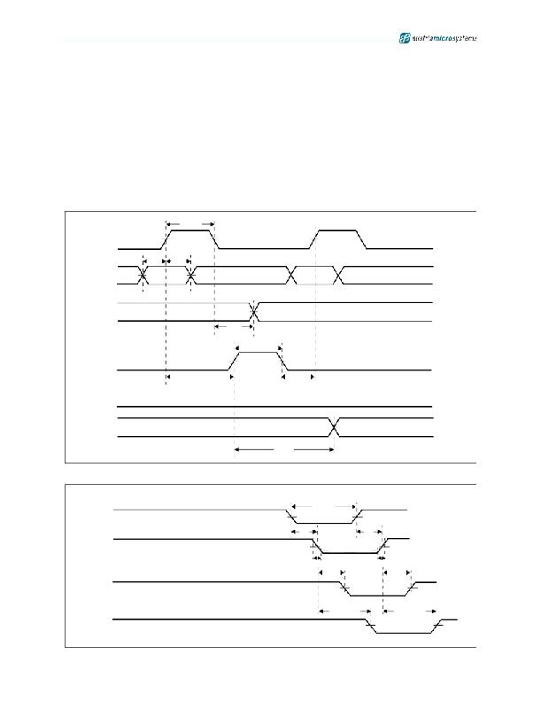
Serial Interface
Data accesses are made serially via pins SDI and SDO. At each CLK rising edge, the signal present at pin SDI is
shifted into the first bit of the internal shift register and the other bits are shifted ahead of the first bit. The MSB is the
first bit to be clocked in. In error-detection mode the shift register will latch-in the corresponding error data of tempera-
ture-, open-, and short-error register with each falling edge of LD.
The 16-bit data register will latch the data of the shift register at each rising edge of LD. This data is then used to drive
the current generator output drivers to switch on the corresponding LEDs as OEN goes low.
Timing Diagrams
This section contains timing diagrams referenced in other sections of this data sheet.
Figure 8. Normal Mode Timing Diagram
t W(CLK)
CLK
SDI
SDO
50%
50%
t SU(D)
t H(D)
50%
50%
50%
50%
t P1
t W(L)
LD
OEN
t SU(L)
50%
50%
t H(L)
OEN Low = Output Enabled
OUTN x
50%
OUTN x High = Output Off
OUTN x Low = Output On
t P2
Figure 9. Output Delay Timing Diagram
t W(OE)
OEN
50%
t P3
90%
50%
t P3
90%
OUTN0
50%
10%
10%
50%
t OF
t STAG
t OR
t STAG
OUTN1
OUTN15
www.austriamicrosystems.com/LED-Driver-ICs/AS1113
Revision 1.04
50%
14 X t STAG
50%
50%
14 X t STAG
50%
9 - 24
发布紧急采购,3分钟左右您将得到回复。
相关PDF资料
AS1117-BQFT
IC DRIVER 64LED MOBILE 24-TQFN
AS1118-BQFT
IC DRIVER 64LED W/DELAY 24-TQFN
AS1121B-BQFT
IC DRIVER 16-CH 32-TQFN
AS1122B-BQFT
IC LED DVR 12-CH 24-TQFN
AS1123-BTST
IC LED DVR 16-CH 40MA 24-QSOP
AS1390A-ZQFT
IC BOOST CTLR/BUCK CONV 20-QFN
AS212-L
SOCKET 12V AUTO SAFETY CAP MNT
AS212C
AUTO 12V SOCKET W/SAFETY CAP
相关代理商/技术参数
AS1113BSSU
制造商:AMS 功能描述:IC LED DRIVER CONSTANT CURRENT SSOP24 制造商:AMS 功能描述:IC, LED DRIVER, CONSTANT CURRENT, SSOP24 制造商:AMS 功能描述:IC, LED DRIVER, CONSTANT CURRENT, SSOP24; Topology:Constant Current; No. of Outputs:16; Output Current:50mA; Output Voltage:15V; Driver Case Style:SSOP; Input Voltage Min:3V; Input Voltage Max:5.5V; Dimming Control Type:Analogue ;RoHS Compliant: Yes
AS1113-BSSU
功能描述:LED显示驱动器 RoHS:否 制造商:Micrel 数位数量:5 片段数量: 安装风格:SMD/SMT 封装 / 箱体:PLCC-44 工作电源电压:4.75 V to 11 V 最大电源电流:10 mA 最大工作温度:+ 85 C 最小工作温度:- 40 C 封装:Tube
AS1113CVB
功能描述:AS1113 - Power Management, Power Over Ethernet (POE) Evaluation Board 制造商:akros silicon 系列:- 零件状态:停产 主要用途:电源管理,以太网供电(POE) 嵌入式:- 使用的 IC/零件:AS1113 主要属性:- 辅助属性:过压,热和欠压保护 所含物品:板 标准包装:1
AS1113-XXX-I-A1-D
制造商:未知厂家 制造商全称:未知厂家 功能描述:Analog Filter
AS1113-XXX-I-A1-S
制造商:未知厂家 制造商全称:未知厂家 功能描述:Analog Filter
AS1113-XXX-I-A2-D
制造商:未知厂家 制造商全称:未知厂家 功能描述:Analog Filter
AS1113-XXX-I-A2-S
制造商:未知厂家 制造商全称:未知厂家 功能描述:Analog Filter
AS1113-XXX-I-A3-D
制造商:未知厂家 制造商全称:未知厂家 功能描述:Analog Filter
